Spectroscopy station
Our spectroscopy station is equipped with a suite of optical probes and a versatile sample environment (temperature, field, strain, pressure). It features the following instrumentation:
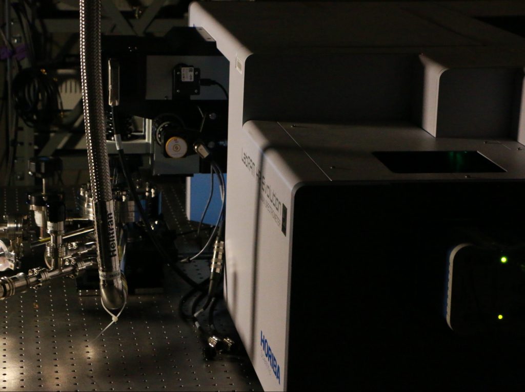
- A high-resolution, high-throughput single-grating Raman spectrometer (Horiba LabRAM HR™) fitted with high-numerical aperture (NA=0.7) microscope objectives and motorized linear stages to perform scanning micro-Raman measurements with ~1 um spot size and minimum Raman shift of 5 cm-1 with <1 cm-1 spectral resolution. Full polarization control on both the incident and scattered beams is achieved using motorized polarizer/analyzer rotators, enabling angle-resolved polarized Raman scattering measurements. The backside of the spectrometer is equipped with two charge-coupled device area detectors with high quantum efficiency and low dark current noise, using thermoelectric cooling (-70 C) and liquid-nitrogen cooling (-120 C), respectively.
- Five laser sources are available for optical experiments: an ultra-narrowband red laser diode (785 nm); an ultra-narrowband green laser diode (532 nm); a HeNe (633nm) source; a 675nm narrowband source tunable over +/- 3nm; and a supercontinuum broadband laser, which is coupled to a monochromator grating providing optical excitation in the range 450-950 nm with subnanometric bandwidth for spectroscopic measurements.
- An optical polarimetry setup with dual modulation/detection scheme (photoelastic modulator + low-noise double lock-in detection; and Wollaston prism + balanced photodiode) that is sensitive to linear polarization rotations and ellipticities down to 50 nanoradians. The polarimeter is designed to permit measurements over the full available optical spectrum available in a single optics set, spanning the near UV to near IR. The magneto-optical Kerr effect is measured in either polar (normal incidence) or longitudinal (30 degree incidence) configurations
- A closed-cycle, low-vibration cryostat (Montana Instruments Cryostation s50™) with 3.5 Kelvin base temperature and two 10-pin electrical feedthroughs including coaxial connections for low-noise electrical measurements.
- A water-cooled electromagnet (Montana Instruments™) delivering a maximum axial field of 1 Tesla (at the sample position).
- An open-flow cryostat (ARS model LT-3-OM UHV™) for special low-temperature experiments down to 4.2 Kelvin in ultra high vacuum.
Diamond anvil cell
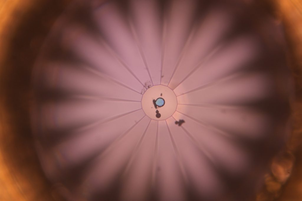
To perform high-pressure experiments at both room temperature and low temperature (< 4 Kelvin), we use a CryoDAC-ST (Almax EasyLab™) high-pressure diamond anvil cell (DAC) that can reach temperatures as low as 4 K and maximum pressures of 50 GPa. This DAC can be mounted in both cryostats for low-temperature optical spectroscopy measurements, including Raman spectroscopy, photoluminescence, reflection contrast and magneto-optical Kerr effect. High-pressure experiments on exfoliated 2D samples use the” horseshoe method” (https://doi.org/10.1016/j.carbon.2020.11.038) that is based on custom-made 70 µm-diameter and 25 µm-thick SiO2/Si substrates. Samples are loaded onto the DAC using a home-built micromanipulator station.
Strain device
Uniaxial strain is a unique perturbation to condensed matter systems, where the lattice parameters can be controllably tuned along selected directions within the crystal. In particular, it has the ability to select lattice distortions within particular symmetry channels and create, promote or suppress rotational symmetry breaking in solids. In our lab, we have two strain cells (Razorbill CS130™) based on piezoelectric stacks for in-situ uniaxial strain tuning at cryogenic temperatures. These are integrated into a 4K cryostat, with magnetic fields up to 0.5 T, and coupled with most optical probes in our toolkit. These strain cells are also used at specialized hard X-Ray beamlines at synchrotron facilities.
Sample synthesis & fab
- Materials’ synthesis
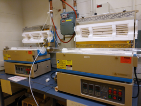
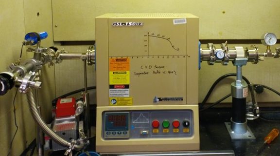
Our lab is equipped with two 3-zone furnaces, two 2-zone furnaces and a box furnace (operating up to 1500 C) to grow crystals via chemical vapor transport and flux method. Additionally, we built a vapor deposition furnace for the bottom-up synthesis of air-sensitive atomically thin 2D materials, including seeded growth on epitaxially-matched substrates. - 2D sample prepation
Samples and devices of 2D materials and heterostructures are prepared inside an Inert Lab 4GB™ glovebox in our lab. We use a motorized transfer setup with integrated optical microscope (5/10x/20/50/100x), a sample XY stage, a transfer XYZR stage (20 nm translation step + 0.2 mrad rotation step) and a vacuum chuck heating stage (150 C). - Device fab
For device fabrication, we use an electron beam lithography tool (Elionix™), housed at MIT-MTL. Lithography is performed by scanning an electron beam over the sample according to an input file, and does not use photomasks. The exposure time is proportional to the pattern area, making the tool ideal for fine features and small total areas. Metal contacts (Au, Ti, Cr, Zr, Ni) are made using an EBeam-AJA™ metal evaporator at MIT.nano. - Atomic force microscopy
Our lab is also equipped with an atomic force microscope (AFM Workshop™) housed inside a homemade glovebox. It is used to perform topographic measurements of air sensitive 2D materials. The AFM has ultra-low noise floor of 20pm, and lateral resolution of 20nm.
Angle-resolved photoemission
Angle-resolved photoemission spectroscopy, or ARPES, is one of the most versatile electronic structure probes in crystalline solids. Using the conservation laws during photoemission process ARPES measures the energy- and momentum-resolved spectral function of electrons, which contains ‘all’ information on how the electrons behave in solid; not only their kinematics but also how they interact with other quasiparticles in solid such as phonons, magnons, plasmons, etc. Consequently, ARPES has played a leading role in the various fields of condensed matter physics ranging from high-temperature superconductors to low-dimensional systems to topological materials.
State-of-art ARPES facilities, commonly based on the third generation synchrotrons, now offer meV energy resolution, sub-micron spatial resolution, photon flux higher than 1012/s, polarization control, cryogenic temperature, and capability to extract the spin information. We are performing ARPES experiments in the cutting-edge ARPES beamlines worldwide including: MAESTRO and MERLIN beamlines in the Advanced Light Source (micro- and nano-ARPES); ESM beamline at the National Synchrotron Light Source II; beamline I05 in the Diamond Light Source (high-resolution ARPES); SIS-COPHEE beamline in the Swiss Light Source (spin-resolved ARPES); BadElph and APE beamlines in the Elettra; and beamline 4A1,2 in the Pohang Light Source.
Optical Test Bench for New Coherent Imaging Methods
Our lab maintains a flexible test bench for developing new coherent imaging methods with applications to optical, x-ray, and electron imaging. The test bench is designed to flexibly accommodate experiments in the transmission, reflection, and Bragg geometries at a variety of wavelengths in the visible spectrum. We have a test fixture which mimics the geometry of a typical soft x-ray diffraction beamline, allowing us to test scale models of novel diffractive optics with applications in coherent x-ray imaging. In addition, we have a microscope-based test fixture which enables optical coherent imaging methods such as vectorial ptychography to be performed at high numerical apertures. These fixtures have enabled us to continue pushing forward the limits of lensless imaging methods, for example in the development of Randomized Probe Imaging and Structured Illumination X-ray Holography.